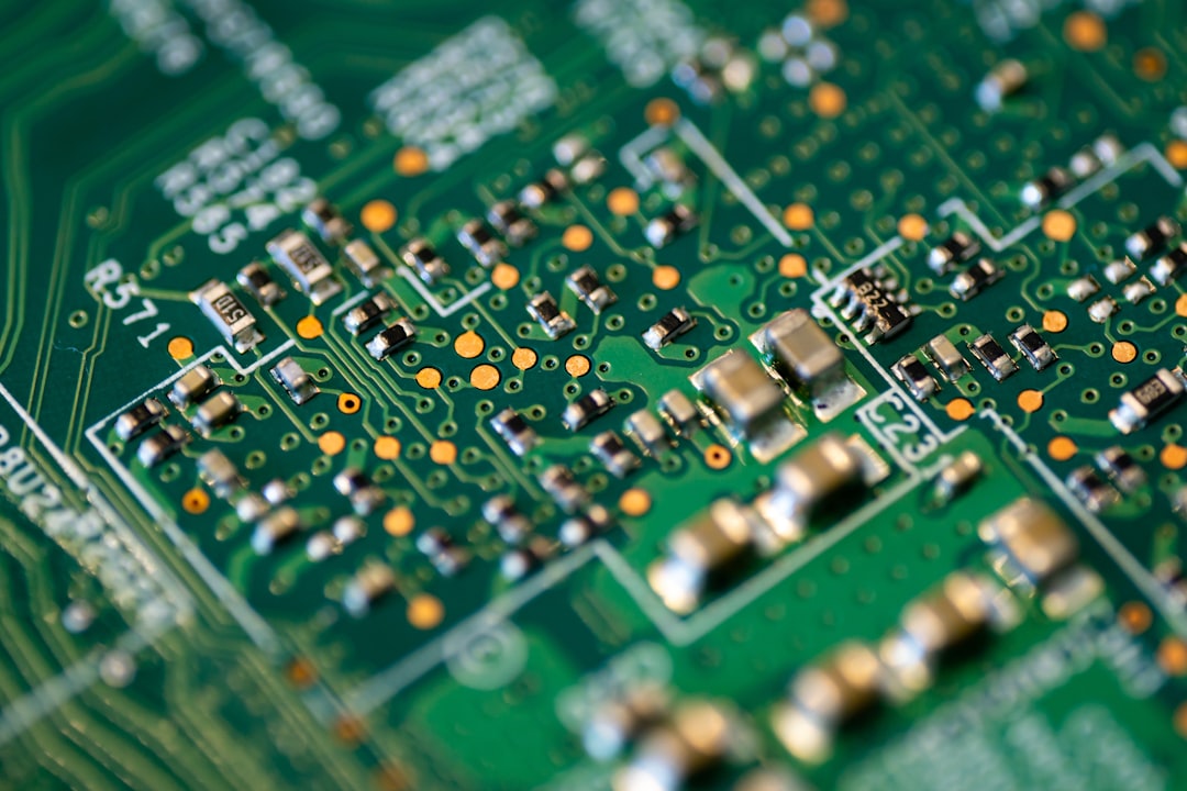
You’re holding a smartphone, a laptop, a smart thermostat. Think about the incredible computing power packed into these devices, the ability to connect to the world, to process information at lightning speed. What makes it all possible? It’s the humble silicon chip, a marvel of modern engineering. But have you ever stopped to wonder how these impossibly complex components are made? You might be surprised to learn that the journey begins with something as common as sand.
From Humble Beginnings: The Raw Material
The story of semiconductor manufacturing is a testament to human ingenuity, transforming a ubiquitous substance into the backbone of our digital age. You see sand everywhere – on beaches, in deserts, in building materials. Most of this sand is composed of silicon dioxide, also known as silica. It’s abundant, inexpensive, and, crucially, possesses the right atomic structure to be the foundation for semiconductor technology. However, not just any sand will do. The silicon dioxide used in semiconductor manufacturing needs to be exceptionally pure.
The Purity Imperative
Think of it like this: imagine trying to build a perfect, flawless crystal. If even a tiny speck of impurity is present, the entire structure can be compromised. In semiconductor manufacturing, even parts per billion of impurities can derail the entire process. Therefore, the first crucial step is sourcing exceptionally pure silicon dioxide. This often involves mining specialized quartz sand deposits, which are naturally richer in silica and have fewer mineral contaminants.
If you’re interested in learning more about the intricate processes involved in the production of semiconductors, you might find this related article insightful: How Semiconductors are Made. This article delves into the various stages of semiconductor manufacturing, including the materials used, the fabrication techniques, and the technologies that drive innovation in this critical industry.
The Alchemical Transformation: Extracting Pure Silicon
Once you’ve identified and sourced the raw material, the real work begins. The silicon dioxide needs to be purified to an incredible degree. This isn’t a simple washing or sifting process; it’s a complex chemical and thermal treatment.
The Carbothermal Reduction: First Steps to Purity
The initial purification stage involves a process called carbothermal reduction. Here, silicon dioxide is heated to very high temperatures in the presence of carbon. The carbon acts as a reducing agent, essentially stripping the oxygen away from the silicon dioxide. This reaction produces a crude form of silicon, often referred to as metallurgical-grade silicon, which is about 98-99% pure. While this might sound pure to you, for semiconductor applications, it’s still far from adequate.
Refining to Electronic Grade: A Quest for Perfection
To achieve the purity required for semiconductors, the metallurgical-grade silicon undergoes further refining. This is where things get truly scientific. One of the most common methods is the Siemens process, which involves converting the silicon into a gaseous compound, typically trichlorosilane (SiHCl3). This gas is then purified through multiple distillation steps, effectively separating the silicon from any remaining impurities.
Distillation Drama: Separating the Good from the Bad
Imagine a complex cocktail where you want to isolate a single ingredient. Distillation is a process that leverages the different boiling points of substances. In this case, the trichlorosilane gas is repeatedly heated and cooled, causing different components to condense and separate. By carefully controlling the temperature and pressure, the impurities, which have different boiling points than trichlorosilane, are selectively removed. This multi-stage distillation is incredibly energy-intensive but absolutely critical for achieving the desired purity.
Deposition and Crystallization: The Birth of the Ingot
Once the trichlorosilane is purified, it’s converted back into solid silicon through a process called chemical vapor deposition (CVD). In this method, the purified gas is passed over heated silicon rods within a special reactor. The gas decomposes, and pure silicon atoms deposit onto the rods, gradually building up a large, crystalline rod of polysilicon. This polysilicon is still not the perfectly ordered crystal needed for advanced chips, but it’s a significant step closer.
The Czochralski Method: Growing the Perfect Crystal
The true birth of a semiconductor wafer begins with the creation of a single-crystal silicon ingot. This is usually achieved using the Czochralski (CZ) method. In this process, a small seed crystal of perfectly structured silicon is dipped into a crucible of molten, ultra-pure polysilicon. The seed crystal is then slowly rotated and pulled upwards. As it’s pulled, the molten silicon solidifies onto the seed, mirroring its crystal structure. This painstakingly slow process ensures that the resulting ingot is a single, continuous crystal lattice of silicon – the perfect foundation for building intricate circuits. These ingots are massive, often several feet long and a foot in diameter, and they are the primary form in which silicon is transported for further processing.
Shaping the Foundation: Wafer Slicing and Polishing
You’ve now got a giant, highly pure, single-crystal silicon ingot. But this ingot is far too large and too rough to be used directly in chip fabrication. The next series of steps involves transforming this massive cylinder into the thin, perfectly flat discs that you know as silicon wafers.
The Precision Cut: Slicing the Ingot
Imagine trying to cut through a loaf of bread with a dull knife. You’d get uneven slices, crumbs everywhere, and it would be a mess. High-precision diamond saws are used to slice the silicon ingot into incredibly thin wafers, typically around 775 micrometers thick (that’s less than a millimeter!). The slicing process needs to be incredibly controlled to minimize stress on the silicon and ensure uniformity.
Sawing Through Stone: The Role of Diamond Blades
The very edges of these saws are embedded with microscopic diamonds. These diamonds are what do the cutting. The process is performed with extreme care, often with a cooling lubricant to prevent overheating and to flush away debris. The speed of the cut, the tension on the blade, and the feed rate of the ingot are all meticulously controlled to achieve wafers of uniform thickness and minimal surface damage.
The Mirror Finish: Grinding and Polishing
Even after slicing, the wafers have microscopic imperfections and are not perfectly flat. They need to be processed to achieve an atomically smooth, mirror-like surface. This involves a series of grinding and polishing steps.
Chemical-Mechanical Planarization (CMP): The Ultimate Smoothing
This is where the magic of achieving an atomically flat surface happens. Chemical-Mechanical Planarization, or CMP, is a sophisticated process that uses a combination of chemical etching and mechanical abrasion. The wafer is placed on a rotating platen covered with a slurry – a mixture of fine abrasive particles and chemicals. As the wafer rotates against this slurry-covered pad, the chemicals soften the silicon surface while the abrasive particles gently polish it away. This process removes surface irregularities with incredible precision, creating a surface so smooth that it’s virtually defect-free at the atomic level. You could, theoretically, look at a perfectly polished silicon wafer under an electron microscope and see nothing but silicon atoms perfectly arranged.
The Art of Circuit Design and Patterning: Imprinting the Blueprint
Now that you have pristine silicon wafers, the stage is set for the most mind-boggling part: creating the intricate circuits that will give the chip its intelligence. This is where design meets manufacturing on an incredibly small scale.
Designing the Brain: Integrated Circuit (IC) Design
Before any manufacturing can begin, the actual design of the chip needs to be conceived. This is the domain of integrated circuit (IC) designers. They use sophisticated Electronic Design Automation (EDA) software to map out every single transistor, every connection, every logic gate on the chip. This design process is incredibly complex, involving billions of transistors on a single chip. The designers think about how information will flow, how power will be distributed, and how the chip will perform its intended function.
From Concept to Code: The Language of Chips
IC designers work with specialized software that allows them to create complex schematics and layouts. Think of it as writing a very detailed blueprint for a microscopic city. This blueprint is then translated into a series of masks – highly precise stencils that will be used to transfer the circuit pattern onto the silicon wafer.
Lithography: Etching the Path
The process of transferring the circuit design onto the wafer is called photolithography. This is arguably the most critical and technically challenging step in semiconductor manufacturing. It’s a process that relies heavily on light to precisely etch patterns onto the silicon.
The UV Kiss: Exposing the Photoresist
First, a light-sensitive chemical called photoresist is applied uniformly to the wafer’s surface. Then, a mask, which contains the pattern for a specific layer of the circuit, is positioned above the wafer. Powerful ultraviolet (UV) light is then shone through the mask. Where the mask is transparent, the UV light strikes the photoresist, causing a chemical change. Where the mask is opaque, the photoresist remains unaffected.
Developing the Image: Revealing the Pattern
After the exposure, the wafer is treated with a developer solution. This solution selectively removes either the exposed or unexposed photoresist, depending on the type of photoresist used. This leaves a patterned layer of photoresist on the wafer, creating a stencil that precisely mirrors the circuit design from the mask.
Understanding how semiconductors are made is crucial for grasping the fundamentals of modern electronics. For those interested in exploring this topic further, you might find a related article on the intricacies of semiconductor manufacturing processes at My Geo Quest. This resource delves into the various stages involved in creating these essential components, shedding light on their significance in today’s technology-driven world.
Building the Layers: Deposition and Etching
With the patterned photoresist in place, you can now begin to build up the layers of the chip and selectively remove material to create the conducting and insulating pathways. This is an iterative process, with many cycles of deposition and etching required to build up the complex three-dimensional structure of a modern chip.
Deposition Techniques: Adding the Building Blocks
Deposition is the process of adding thin layers of various materials onto the wafer. These materials can be conductors (like copper or aluminum), insulators (like silicon dioxide or silicon nitride), or semiconductors themselves.
Chemical Vapor Deposition (CVD): Building from Gases
CVD is a widely used technique where gaseous precursors are introduced into a reaction chamber. These gases react on the wafer surface, depositing a thin, uniform film of the desired material. This is a very precise way to create thin films with controlled properties.
Physical Vapor Deposition (PVD): Sputtering with Precision
PVD, often referred to as sputtering, involves bombarding a target material with energized ions. This dislodges atoms from the target, which then deposit onto the wafer. This method is excellent for depositing metals and other conductive materials.
Etching: Sculpting the Circuits
Etching is the counterpart to deposition. It’s the process of selectively removing material from the wafer.
Dry Etching: Plasma Power
In dry etching, a plasma – an ionized gas – is used to chemically react with and remove the exposed material. This process is highly directional and allows for the creation of very fine features.
Wet Etching: Chemical Baths
Wet etching uses liquid chemicals to selectively dissolve away unwanted material. While less precise than dry etching for very small features, it’s still a valuable technique for certain applications.
The Final Touches: Interconnections and Testing
You’ve now built up layers of meticulously patterned conductors and insulators on your silicon wafer. But the individual transistors and components are still isolated. The next steps are about connecting them all together and ensuring that everything works as intended.
Metallization: The Tiny Roads
To connect the thousands, millions, or even billions of transistors, intricate networks of metal lines are created. This process is called metallization. Multiple layers of metal, typically copper for high-performance chips, are deposited and patterned using photolithography and etching. These metal lines act as the “roads” that carry electrical signals across the chip.
The Rise of Copper: Efficiency and Speed
Copper has largely replaced aluminum in modern chips because of its lower electrical resistance. This means that electrical signals can travel faster and with less power loss, leading to more powerful and efficient chips. However, copper is also more prone to diffusion, requiring sophisticated barrier layers to prevent it from migrating into the surrounding silicon.
Testing and Packaging: Ready for the World
Once the entire circuit is etched and connected on the wafer, each individual chip needs to be tested to ensure it functions correctly.
Wafer Sort: Identifying the Winners
First, a process called wafer sort is performed. Using automated probes, each individual die (the small rectangular or square chip on the wafer) is electrically tested. Any die that fails these tests is marked and will be discarded later. You’re aiming for incredibly high yields, but some defects are inevitable at this scale.
Dicing and Packaging: From Wafer to Component
The wafer is then cut, or “diced,” into individual chips using a diamond saw. These individual good dies are then mounted onto a substrate – a small circuit board that provides electrical connections to the outside world. This entire assembly is then enclosed in a protective package, which is what you typically see as the black component with pins or solder balls. This packaging protects the delicate silicon chip from physical damage and environmental factors, and it provides the interface for connecting the chip to other components on a larger circuit board.
And there you have it. From a handful of sand, through a series of incredibly complex and precise chemical and physical processes, you’ve arrived at the silicon chip that powers your modern world. It’s a testament to human ingenuity, precision engineering, and an unwavering pursuit of perfection at the atomic level. The next time you pick up your phone, take a moment to appreciate the incredible journey of that tiny, powerful piece of silicon. You’ve witnessed the transformation of the mundane into the magical.

The Taiwan Strait: The Most Dangerous Place in the Global Economy
FAQs
What are semiconductors made of?
Semiconductors are typically made of materials such as silicon, germanium, and gallium arsenide. These materials have properties that allow them to conduct electricity under certain conditions.
How are semiconductors manufactured?
The manufacturing process of semiconductors involves several steps, including crystal growth, wafer fabrication, and device processing. These steps require precise control and high levels of cleanliness to ensure the quality of the final product.
What is the role of doping in semiconductor production?
Doping is the process of intentionally introducing impurities into a semiconductor material to alter its electrical properties. This is a crucial step in semiconductor production as it allows for the creation of p-type and n-type semiconductors, which are essential for building electronic devices.
What is the significance of cleanroom environments in semiconductor manufacturing?
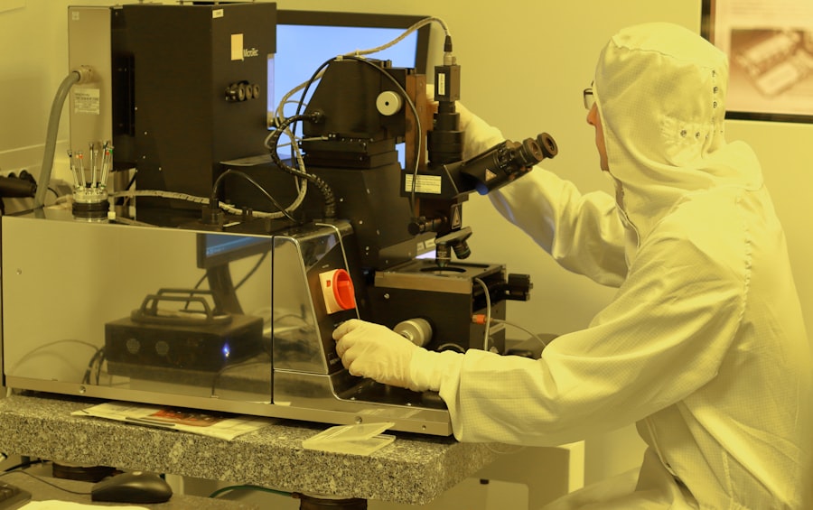
Cleanroom environments are essential in semiconductor manufacturing to prevent contamination of the materials and ensure the quality and reliability of the final product. These environments have strict controls for air quality, temperature, and humidity to minimize the presence of particles and other contaminants.
What are some common applications of semiconductors?
Semiconductors are used in a wide range of electronic devices, including transistors, diodes, integrated circuits, and solar cells. They are also essential components in various industries such as telecommunications, automotive, and consumer electronics.