You’re probably surrounded by them right now, maybe even reading this on one. They’re in your phone, your car, your smart fridge, and the cloud servers humming away behind the screens you depend on. Semiconductors, those tiny chips that power our modern world, are indispensable. But you’ve heard the news, haven’t you? The constant chatter about shortages, delays, and geopolitical tensions. It’s not just a headline; it’s a palpable reality impacting businesses and consumers alike. Navigating the semiconductor supply chain is no longer a niche concern for industry insiders; it’s a strategic imperative for anyone looking to understand and thrive in the current economic landscape.
This intricate web of manufacturing, materials, and logistics is a marvel of human ingenuity, but it’s also incredibly vulnerable. From the raw silicon extracted from sand to the complex fabrication plants that etch microscopic patterns onto wafers, each step is critical. And when one link in this chain falters, the ripple effects can be profound and far-reaching. Understanding these dynamics is key to anticipating challenges, mitigating risks, and ultimately, securing the technology that underpins our lives.
The semiconductor supply chain is not a single entity but a vast, interconnected ecosystem. Imagine a meticulously orchestrated symphony, where each instrument plays a vital role, and any disruption to one can throw the entire performance off-key. To truly navigate this complexity, you first need to appreciate its constituent parts.
From Sand to Silicon: The Raw Material Foundation
It all begins with something as mundane as sand, specifically quartz sand, which is rich in silicon dioxide. This seemingly simple ingredient undergoes a transformative journey to become the ultra-pure silicon that forms the foundation of every semiconductor.
Extracting and Purifying Quartz
The process starts with mining high-purity quartz. This isn’t just any beach sand; it requires specific geological deposits with low levels of impurities. The mined quartz is then crushed and subjected to intense heat in electric arc furnaces. This melts the silicon dioxide, and through a series of chemical reactions, separates the silicon from the oxygen. The result is metallurgical-grade silicon, which is still impure by semiconductor standards.
The Quest for Semiconductor-Grade Purity
Achieving the incredible purity required for microchips – often 99.9999999% pure or higher – is a monumental feat. This is typically done through a process called the Siemens process or the Fluidized Bed Reactor (FBR) process. These methods involve reacting the impure silicon with chemicals like hydrogen chloride to form trichlorosilane, a volatile liquid. This trichlorosilane is then distilled multiple times to remove impurities. Finally, the purified trichlorosilane is decomposed onto heated silicon rods, depositing layers of hyper-pure polycrystalline silicon. This is the raw material for the next critical stage.
The semiconductor supply chain has been a focal point of discussion in recent years, particularly due to its impact on global technology markets. For a deeper understanding of the challenges and developments within this sector, you can read a related article that explores the intricacies of the semiconductor supply chain and its implications for various industries. Check it out here: Semiconductor Supply Chain Insights.
The Art of Wafer Fabrication: Where Magic Happens
This pure silicon then embarks on the most intricate and expensive part of its journey: wafer fabrication. This is where microchips are actually created, designed, and manufactured.
Growing Silicon Ingots and Slicing Wafers
The polycrystalline silicon is melted and slowly pulled into a single, perfect cylindrical crystal called an ingot. This is done using techniques like the Czochralski process. These ingots, which can be over two meters long, are then precisely sliced into thin, circular wafers, typically with diameters of 200mm or 300mm. These wafers are the canvases upon which countless integrated circuits will be etched.
Photolithography: The Art of Patterning
The heart of wafer fabrication lies in photolithography. This is a complex process that uses light to transfer intricate circuit designs from a mask onto the silicon wafer. Layers of light-sensitive material, called photoresist, are applied to the wafer. Then, ultraviolet light is shone through a mask – a stencil containing the chip’s design – onto the photoresist. The exposed areas of photoresist harden, while the unexposed areas can be washed away, creating a pattern. This process is repeated hundreds of times, layering different materials and etching away unwanted portions to build up the three-dimensional circuitry of the chip.
The complexities of the semiconductor supply chain have become increasingly evident in recent years, especially as global demand continues to surge. For those interested in understanding the intricacies of this vital industry, a related article can provide valuable insights. You can explore more about the challenges and innovations shaping the semiconductor landscape by visiting this informative resource. This article delves into the factors influencing supply chain dynamics and offers a comprehensive overview of the current state of the semiconductor market.
Etching and Doping: Shaping the Circuits
After photolithography defines the pattern, etching is used to remove unwanted silicon or deposited layers. This can be done using wet chemicals or plasma etching, which bombards the wafer with reactive ions. Doping, on the other hand, involves introducing impurities into specific regions of the silicon to alter its electrical conductivity. This is crucial for creating the transistors and other components that make up a chip. This intricate dance of deposition, photolithography, etching, and doping happens within ultra-clean room environments, where even a single dust particle can ruin an entire batch of chips.
Packaging and Testing: The Final Touches
Once the intricate circuitry is formed on the wafer, the individual chips need to be prepared for their end use. This involves cutting the wafer into individual dies and then packaging them.
Dicing the Wafer: Separating the Dies
The wafer, now covered in hundreds or even thousands of identical chips (dies), is cut into individual pieces using a precision saw or laser. Each of these dies is a functional semiconductor chip.
Wire Bonding and Encapsulation: The Protective Shell
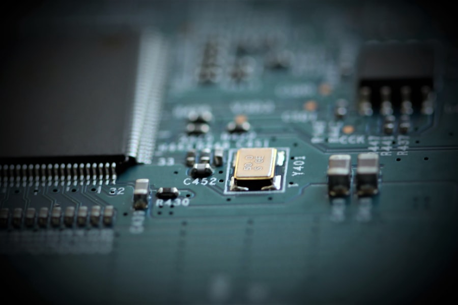
Next, the individual dies are attached to a substrate, typically a small circuit board. Tiny wires, bonded to contact points on the die and the substrate, connect the chip to the outside world. The entire assembly is then encapsulated in a protective plastic or ceramic casing, shielding the delicate circuitry from physical damage and the environment. This is the familiar black rectangular component you often see on circuit boards.
Rigorous Testing: Ensuring Functionality
Before any chip can be shipped, it undergoes extensive testing. This involves checking each chip for functionality, performance, and reliability to ensure it meets the required

The Taiwan Strait: The Most Dangerous Place in the Global Economy
FAQs
What is a semiconductor supply chain?
A semiconductor supply chain refers to the network of companies and processes involved in the production and distribution of semiconductors, which are essential components in electronic devices.
What are the key components of a semiconductor supply chain?
The key components of a semiconductor supply chain include raw material suppliers, semiconductor manufacturers, assembly and testing companies, and distributors.
Why is the semiconductor supply chain important?
The semiconductor supply chain is important because semiconductors are critical components in a wide range of electronic devices, including smartphones, computers, and automotive systems. Any disruptions in the supply chain can impact the availability and cost of these devices.
What are some challenges in the semiconductor supply chain?
Challenges in the semiconductor supply chain include supply shortages, geopolitical tensions affecting trade, and the complexity of coordinating production and distribution across multiple companies and regions.
How does the semiconductor supply chain impact the global economy?
The semiconductor supply chain has a significant impact on the global economy, as it affects the production and availability of electronic devices that are essential for various industries and consumer markets. Disruptions in the supply chain can lead to economic repercussions worldwide.