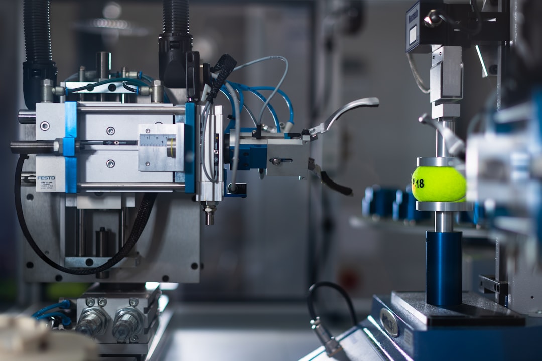
You stand at the precipice of an era defined by unparalleled technological advancement, an era where the very building blocks of the digital world are being sculpted with ever-increasing precision. Semiconductor manufacturing, the intricate dance of atoms and light that underpins our modern existence, is not a static field. It’s a relentless current, constantly pushing the boundaries of what’s possible, and you, as a discerning observer or active participant, are witnessing this evolution firsthand. You’re experiencing the drive towards smaller, faster, and more powerful chips, a journey fraught with immense challenges but also brimming with groundbreaking solutions.
You understand that for decades, the semiconductor industry has been guided by Moore’s Law, a prediction that the number of transistors on a microchip doubles approximately every two years. While this exponential growth has fueled the digital revolution, you also recognize that maintaining this pace is becoming increasingly difficult. The physical limitations of silicon are being stretched to their absolute limits.
Lithography: The Art of Patterning at the Nanoscale
You know that lithography is the cornerstone of semiconductor manufacturing, the process of transferring circuit patterns onto silicon wafers. For years, Deep Ultraviolet (DUV) lithography has been the workhorse, utilizing wavelengths of light to etch intricate designs. However, as feature sizes shrink, DUV’s resolution becomes insufficient.
Extreme Ultraviolet (EUV) Lithography: The New Frontier
Your attention is drawn to Extreme Ultraviolet (EUV) lithography, a game-changer that utilizes light with a much shorter wavelength (13.5 nanometers). This allows for the patterning of incredibly small features, enabling the creation of transistors that are significantly more densely packed. You see the immense complexity of EUV systems – the highly reflective multilayer mirrors, the powerful laser-produced plasma sources, and the vacuum environments required. The development and implementation of EUV represent a monumental leap, pushing manufacturing capabilities into entirely new territory. You understand that the cost and complexity of EUV are significant, but the payoff in terms of performance and miniaturization is undeniable.
Multi-patterning Techniques: Extending DUV’s Lifespan
Even with the advent of EUV, you are aware that older DUV techniques are not entirely obsolete. Multi-patterning strategies, such as Double Patterning and FinFET (Fin Field-Effect Transistor) structures, have been crucial in squeezing more density out of existing DUV processes. You recognize that these techniques involve multiple lithography and etching steps to define a single layer, increasing process complexity and cost but effectively extending the life of DUV technology for certain critical layers.
New Materials and Architectures: Breaking Free from Silicon’s Constraints
You appreciate that the pursuit of miniaturization isn’t solely about refining existing technologies; it also involves exploring entirely new materials and architectural designs. Silicon, while incredibly versatile, has inherent limitations.
High-k Dielectrics and Metal Gates: Improving Transistor Performance
You observe the evolution of transistors themselves. The insulating layer (dielectric) and the gate electrode are critical components. You see the transition from traditional silicon dioxide dielectrics and polysilicon gates to high-k dielectrics (materials with a higher dielectric constant) and metal gates. This innovation allows for thinner gate dielectrics without increased leakage current, leading to better electrostatic control over the transistor channel and improved performance. You understand that the introduction of new materials requires a deep understanding of their electrical properties and their compatibility with existing manufacturing processes.
3D Architectures: Stacking Functionality
Your gaze shifts to the vertical dimension. You witness the move from planar transistors to three-dimensional (3D) structures like FinFETs and, more recently, Gate-All-Around (GAA) transistors. In FinFETs, the gate wraps around the channel like a fin, providing superior control. GAA takes this a step further, with the gate encircling the channel entirely, offering even better performance and reduced leakage. You grasp the manufacturing challenges associated with these 3D structures, including the precise etching and deposition required to create these intricate geometries. The ability to stack transistors in three dimensions unlocks new possibilities for increasing density and power efficiency without solely relying on shrinking lateral dimensions.
Advanced semiconductor manufacturing is a rapidly evolving field that plays a crucial role in the development of modern technology. For those interested in exploring this topic further, a related article can be found at MyGeoQuest, which delves into the latest advancements and innovations in semiconductor technology, highlighting their impact on various industries and the future of electronics.
Enhancing Yield and Reliability: The Unsung Heroes of Production
You know that building the most advanced chips is only half the battle. Ensuring that a vast majority of these chips function flawlessly – high yield – and perform reliably over their intended lifespan is paramount. This involves a multifaceted approach encompassing process control, defect detection, and advanced testing methodologies.
Metrology and Inspection: The Eyes of the Factory
You understand that you can’t improve what you can’t measure. Metrology and inspection technologies are the eyes and ears of the semiconductor factory, constantly monitoring every stage of the manufacturing process. You see advanced tools using optical microscopy, electron microscopy, X-rays, and even acoustic waves to detect and characterize defects at the atomic level.
In-Line Metrology: Catching Problems Early
Your focus sharpens on in-line metrology, where measurements are taken directly during the manufacturing process. This allows for immediate identification of deviations from desired parameters, enabling corrective actions before entire batches of wafers are compromised. You realize the immense data generated by these systems and the crucial role of advanced data analytics and machine learning in interpreting this information effectively.
Wafer Inspection: Spotting Microscopic Flaws
You witness the relentless inspection of wafers for any anomalies. Even microscopic particles or subtle variations in film thickness can lead to catastrophic failures. You see the sophisticated algorithms employed to differentiate between critical defects and benign variations, ensuring that costly production downtime is minimized.
Advanced Packaging: Beyond the Chip
You recognize that the performance and functionality of electronic devices are not solely determined by the chip itself, but also by how it’s packaged and integrated with other components. Advanced packaging techniques are increasingly vital for bridging the gap between shrinking chip technology and the demands of complex systems.
Chiplets and Heterogeneous Integration: Building Blocks for Complexity
Your perspective broadens to encompass the concept of chiplets. Instead of fabricating a monolithic, massive chip, you see the trend towards breaking down complex functionalities into smaller, specialized “chiplets.” These chiplets are then integrated together within a single package. This approach offers significant advantages, including improved yield (as smaller individual components are easier to manufacture successfully), heterogeneous integration (combining different types of chiplets built with different processes), and flexibility in system design. You are learning about advanced interconnect technologies like 2.5D and 3D packaging that enable these chiplets to communicate at extremely high speeds.
Fan-Out Wafer-Level Packaging (FOWLP): Enhanced Connectivity
You observe the advancements in Fan-Out Wafer-Level Packaging (FOWLP), a technology that allows for more input/output (I/O) connections per chip and greater flexibility in die size and shape. This packaging method goes beyond traditional methods by embedding the interconnections beneath the chip, rather than having them solely on the substrate. You understand that FOWLP is contributing to smaller, thinner, and more powerful devices.
Automation and Digitalization: The Smart Factory Revolution
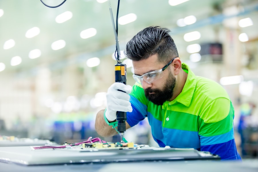
You understand that the sheer complexity and scale of modern semiconductor manufacturing necessitate a high degree of automation and digitalization. The “smart factory” is no longer a futuristic concept; it’s a present-day reality, transforming how chips are made.
Advanced semiconductor manufacturing is a rapidly evolving field that plays a crucial role in the development of modern technology. For those interested in exploring this topic further, a related article can be found at this link, which delves into the latest innovations and challenges in the semiconductor industry. Understanding these advancements is essential for anyone looking to grasp the future of electronics and computing.
Robotics and Automated Material Handling: Precision and Efficiency
Your eyes follow the seamless movement of robotic arms and automated guided vehicles (AGVs) within the cleanroom. You witness the intricate ballet of robots handling delicate wafers with precision, transporting them between different processing stations. This automation minimizes human intervention, reducing the risk of contamination and human error, while simultaneously increasing throughput and efficiency. You see how these systems are meticulously controlled to ensure every step is executed flawlessly.
Artificial Intelligence (AI) and Machine Learning (ML): Driving Smarter Decisions
You acknowledge the growing influence of AI and ML in semiconductor manufacturing. You see these technologies being deployed to analyze the massive datasets generated by metrology and inspection tools, identifying patterns and anomalies that might be imperceptible to human operators. You are witnessing AI-powered systems optimizing process parameters in real-time, predicting equipment failures before they occur, and even assisting in the design of new manufacturing processes. This data-driven approach is leading to faster problem-solving, improved yield, and more consistent production.
Predictive Maintenance: Minimizing Downtime
You grasp the concept of predictive maintenance, where AI algorithms analyze sensor data from manufacturing equipment to predict potential failures. This allows for scheduled maintenance before a critical component breaks down, drastically reducing costly unexpected downtime. You understand that this shift from reactive to proactive maintenance is a cornerstone of efficient factory operations.
Process Optimization: Fine-Tuning for Peak Performance
You observe how ML models are being trained on historical production data to identify the optimal settings for each manufacturing step. This continuous fine-tuning leads to higher yields, reduced waste, and improved overall process stability. You see that the goal is to create a self-optimizing manufacturing environment.
Emerging Technologies and Future Directions: Charting the Next Horizon
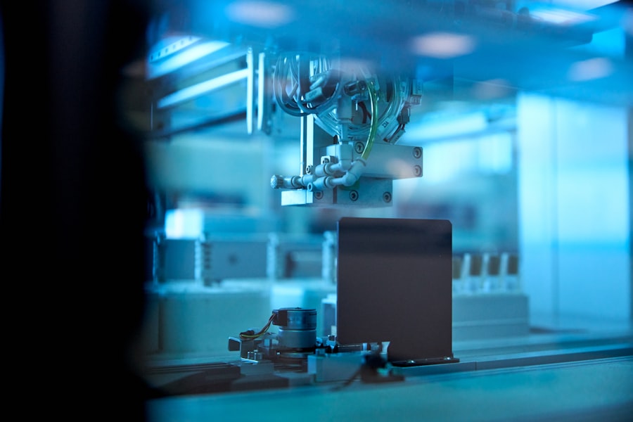
You understand that the landscape of semiconductor manufacturing is perpetually evolving, with researchers and engineers constantly exploring new frontiers. The challenges of today are the stepping stones to the innovations of tomorrow.
Beyond Silicon: Exploring New Semiconductor Materials
Your curiosity is piqued by the exploration of materials beyond silicon. You are learning about the potential of gallium nitride (GaN) and silicon carbide (SiC) for high-power electronics, offering advantages in efficiency and heat dissipation. You see the ongoing research into new semiconductor materials with exotic properties that could unlock entirely new classes of devices. You understand that transitioning to new materials involves significant research and development, including the creation of new fabrication processes and the qualification of these materials for mass production.
Quantum Computing and Neuromorphic Computing: Demanding New Manufacturing Paradigms
You are aware that emerging computational paradigms like quantum computing and neuromorphic computing will require entirely new approaches to semiconductor design and manufacturing. Quantum computers, for instance, rely on delicate quantum states that demand extremely precise fabrication and novel materials. Neuromorphic chips, designed to mimic the human brain, require intricate interconnections and specialized learning mechanisms that challenge current manufacturing capabilities. You understand that the development of these future technologies is intrinsically linked to the advancements you are witnessing in the present.
Substrate Engineering: Tailoring the Foundation
You recognize that the base material, the substrate, is becoming increasingly important. You are learning about the development of new substrate materials and techniques to enhance thermal management, improve electrical isolation, and overcome limitations of traditional silicon. This could involve advanced substrates for specialized applications or novel ways to integrate different materials.
Sustainable Manufacturing: A Growing Imperative
You understand that the environmental impact of manufacturing is a critical concern. You see a growing emphasis on developing more sustainable semiconductor manufacturing processes. This includes reducing energy consumption, minimizing hazardous chemical usage, and improving recycling and waste management practices. You believe that innovation in this area will be just as crucial as advancements in performance and miniaturization. You see a future where efficiency and environmental responsibility go hand-in-hand, driving the next wave of innovation.
You are witnessing a revolution, a constant push and pull between theoretical possibility and practical implementation. The intricate world of semiconductor manufacturing is a testament to human ingenuity and perseverance, a field where every infinitesimally small advancement paves the way for a more connected, intelligent, and capable future. You are part of this exciting journey, and the journey is far from over.

The Taiwan Strait: The Most Dangerous Place in the Global Economy
FAQs
What is advanced semiconductor manufacturing?
Advanced semiconductor manufacturing refers to the process of creating integrated circuits and other semiconductor devices using cutting-edge technology and techniques. This includes processes such as lithography, etching, deposition, and doping to create complex and high-performance semiconductor devices.
What are some key technologies used in advanced semiconductor manufacturing?
Some key technologies used in advanced semiconductor manufacturing include extreme ultraviolet (EUV) lithography, 3D packaging, FinFET transistors, and advanced materials such as high-k metal gate (HKMG) and silicon-on-insulator (SOI) technologies.
What are the benefits of advanced semiconductor manufacturing?
Advanced semiconductor manufacturing allows for the creation of smaller, faster, and more power-efficient semiconductor devices. This enables the development of advanced electronics such as smartphones, computers, and IoT devices, as well as emerging technologies like artificial intelligence and 5G.
What are some challenges in advanced semiconductor manufacturing?
Challenges in advanced semiconductor manufacturing include the high cost of equipment and materials, the complexity of integrating new technologies, and the need for highly skilled engineers and technicians. Additionally, ensuring the reliability and quality of advanced semiconductor devices is a significant challenge.
What is the future outlook for advanced semiconductor manufacturing?
The future of advanced semiconductor manufacturing is expected to involve continued innovation in technologies such as EUV lithography, 3D packaging, and advanced materials. Additionally, there is a growing focus on sustainability and environmental impact, as well as the development of new applications for semiconductor devices in areas such as automotive, healthcare, and renewable energy.