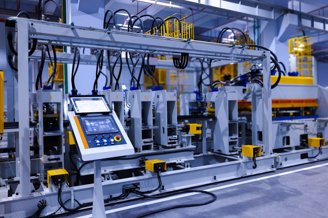
You stand on the precipice of a technological revolution, and at its heart lies something incredibly small, yet astonishingly powerful: the microchip. You’ve seen its manifestations everywhere, from the smartphone in your pocket to the airplane soaring through the sky, the medical equipment saving lives, and the complex AI systems shaping our future. This ubiquitous silicon marvel, packed with billions of microscopic transistors, is the brain of our digital world. But have you ever stopped to think about how these intricate circuits are brought to life? The advancements in microchip manufacturing are not just incremental; they are seismic shifts, pushing the boundaries of physics, engineering, and material science at an unprecedented pace. You are witnessing a story of miniaturization, precision, and innovation that is fundamentally rewriting the rules of what’s possible.
The very foundation of microchip creation rests on a process you might not fully appreciate: photolithography. This is where the blueprints of your chip, the intricate patterns of its circuits, are etched onto silicon wafers. For decades, this has been the workhorse of the industry, but even here, remarkable advancements are being made, enabling you to shrink circuits to previously unimaginable scales.
Extreme Ultraviolet (EUV) Lithography: A Quantum Leap
Perhaps the most significant recent advancement you’re seeing is the widespread adoption and maturation of Extreme Ultraviolet (EUV) lithography. This isn’t just a minor upgrade; it’s a fundamental paradigm shift in how we print these microscopic patterns.
The Wavelength Revolution
Traditionally, photolithography used visible or deep ultraviolet (DUV) light with wavelengths of around 248nm or 193nm. While effective for many years, as you push for smaller transistors, these wavelengths become too large, leading to diffraction effects that blur the intricate designs. EUV lithography changes the game by employing light with a wavelength of just 13.5nm. This minuscule wavelength allows for the printing of much finer features, enabling the creation of denser and more powerful chips. Your current generation of smartphones, for instance, owe their incredible performance to the integration of EUV-fabricated components.
The Technological Hurdles Overcome
Achieving this leap wasn’t easy. EUV light is absorbed by almost everything, including air. This meant a complete reimagining of the lithography tools. You needed to operate in a vacuum, use highly reflective multi-layer mirrors (instead of lenses which would absorb the light), and develop entirely new light sources. These sources are incredibly complex, often involving blasting molten tin droplets with a powerful laser to generate the EUV photons. The engineering required to control and focus this energetic plasma is nothing short of astonishing, a testament to human ingenuity.
The Impact on Moore’s Law
For years, Moore’s Law, the observation that the number of transistors on a microchip doubles approximately every two years, has been a driving force in the industry. EUV lithography is a critical enabler for continuing this trend. By allowing for smaller transistors and more intricate designs, it directly contributes to increased transistor density, which in turn leads to more powerful, energy-efficient, and cost-effective chips. You are living in an era where Moore’s Law, once thought to be nearing its end, is being revitalized thanks to these lithographic advancements.
Advanced Masking and Reticle Technologies
Beyond the light source itself, the masks – the templates that contain the circuit patterns – have also seen significant innovation.
Multi-Patterning Techniques and their Evolution
Before EUV became a widespread reality, the industry relied heavily on multi-patterning techniques to achieve smaller feature sizes. This involved printing a single layer of the chip’s design in multiple steps, using different masks and etching processes. While effective, these methods were complex, time-consuming, and prone to overlay errors, where the precision of aligning each printed layer became critical. EUV significantly simplifies this, often allowing for single-pass patterning for many critical layers, thereby improving yield and efficiency.
Defects, Detection, and Correction
The sheer scale of miniaturization means that even the smallest defect on a mask or wafer can render a chip useless. Therefore, advanced inspection and repair technologies are paramount. You’re seeing the development of highly sensitive optical and electron-beam inspection systems that can detect defects at the nanometer scale. Furthermore, sophisticated repair techniques, often involving focused ion beams or laser-based methods, are employed to fix minor imperfections on masks, ensuring the integrity of the printed patterns.
Microchip manufacturing is a critical component of the technology industry, influencing everything from consumer electronics to automotive systems. For a deeper understanding of the challenges and innovations in this field, you can read a related article that explores the latest advancements and trends in microchip production. Check it out here: Microchip Manufacturing Insights.
The Art of the Etch: Precision in Three Dimensions
Once the pattern is transferred via photolithography, the next crucial step is etching away unwanted material to form the intricate three-dimensional structures of the chip. This isn’t a brute-force removal; it’s a highly controlled, nanoscale sculpting process.
Plasma Etching Advancements
Plasma etching, where reactive ions in a plasma state are used to selectively remove material, is the workhorse of this process. However, the demands for ever-smaller features and more complex 3D structures have driven significant innovations.
Directional Etching and Anisotropy Control
The key to creating sharp, well-defined features lies in achieving highly directional etching, known as anisotropic etching. This means the etching process removes material primarily in one direction (vertically) rather than isotropically (in all directions). Modern plasma etching techniques utilize precisely controlled ion bombardment and chemical reactions to achieve this, ensuring that sidewalls are nearly perpendicular, preventing feature collapse and enabling tighter packing of transistors.
Atomic Layer Etching (ALE): Unprecedented Control
For the most critical and delicate features, Atomic Layer Etching (ALE) has emerged as a game-changer. Unlike traditional plasma etching, ALE works by alternately exposing the wafer to specific reactants in self-limiting surface reactions. This means that in each cycle, only a single atomic layer of material is removed. This level of atomic-scale precision is essential for creating ultra-thin gate dielectrics, tightly controlled vias, and other nanoscale features that are crucial for advanced transistor designs. Your future chips will benefit immensely from the fine-tuning that ALE provides.
Wet Etching and Chemical Mechanical Planarization (CMP)
While plasma etching dominates for many critical processes, wet etching and CMP still play vital roles in shaping the chip’s landscape.
Selective Wet Etching
Advancements in chemical formulations have led to the ability to selectively etch different materials with high precision. This is crucial for removing sacrificial layers or cleaning surfaces without damaging sensitive underlying structures. You’re seeing the development of “greener” chemistries that are more environmentally friendly while maintaining high performance.
CMP for a Flat Surface
As chip layers become more complex and stacked, maintaining a perfectly flat surface is essential for subsequent processing steps. Chemical Mechanical Planarization (CMP) uses a combination of chemical action and mechanical polishing to achieve this. Modern CMP slurries and polishing pads are engineered with incredible precision to remove material uniformly across the wafer, ensuring that subsequent lithography and etching steps can be performed with the required accuracy. You can think of CMP as the meticulous sanding and polishing that leads to a perfect canvas for the next intricate design.
The Tiny Towers: Advances in Deposition Techniques

Building up the intricate circuitry of a microchip involves depositing ultrathin layers of various materials – conductors, insulators, and semiconductors – with atomic precision. The methods you’re using today are far more sophisticated than those of a decade ago.
Chemical Vapor Deposition (CVD) and its Evolution
Chemical Vapor Deposition (CVD) is a ubiquitous technique where gaseous precursors react on a heated substrate surface, depositing a solid film. This process has undergone significant refinement.
Atomic Layer Deposition (ALD): The Ultimate Precision Tool
Similar to ALE in its atomic-scale control, Atomic Layer Deposition (ALD) is a critical technique for depositing ultrathin, conformal films with exceptional uniformity. ALD operates through sequential, self-limiting surface reactions. This means you can deposit films with thicknesses of just a few atoms, ensuring perfect coverage even in the most complex 3D structures. This is crucial for creating high-k dielectric layers in transistors and for forming passivation layers that protect the chip from environmental degradation. You can imagine ALD as painting with atoms, layer by exquisite layer.
Plasma-Enhanced CVD (PECVD) and other Variants
Plasma-Enhanced CVD (PECVD) offers the advantage of allowing deposition at lower temperatures, which is crucial for substrates that cannot withstand high heat. There are also other specialized CVD techniques, such as Metal-Organic CVD (MOCVD) used for specific compound semiconductor applications, each tailored to the unique requirements of different materials and chip architectures.
Physical Vapor Deposition (PVD) and Sputtering Innovations
Physical Vapor Deposition (PVD) techniques, such as sputtering, involve physically transferring material from a target to the substrate. While older, these methods are continuously being improved.
High-Throughput Sputtering
Advancements in sputtering targets, magnetron configurations, and vacuum system design have led to significantly higher deposition rates and improved film uniformity. This is critical for high-volume manufacturing, where efficiency and throughput are paramount.
Reactive Sputtering for Complex Materials
Reactive sputtering allows for the deposition of complex compounds by introducing reactive gases into the sputtering chamber. This technique is vital for creating various oxides, nitrides, and other functional materials that are essential components of modern microchips.
The Backbone of Functionality: New Materials and Architectures
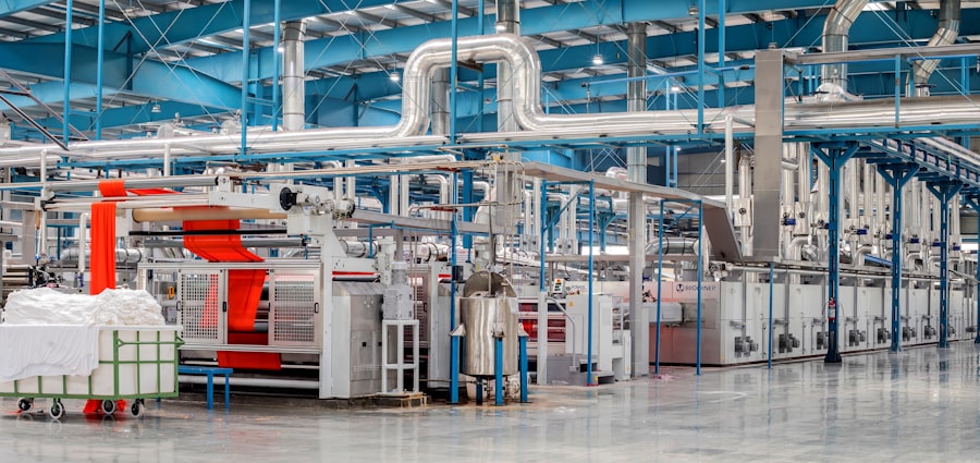
The relentless pursuit of performance and efficiency in microchips isn’t just about refining existing processes; it’s also about exploring and integrating entirely new materials and reimagining chip architectures.
Beyond Silicon: Emerging Semiconductor Materials
While silicon has been the undisputed king of semiconductors for decades, limitations in its performance are driving the exploration of alternative materials.
Gallium Nitride (GaN) and Silicon Carbide (SiC)
Gallium Nitride (GaN) and Silicon Carbide (SiC) are two materials that are rapidly gaining prominence, particularly for high-power and high-frequency applications. They offer superior performance in terms of breakdown voltage, thermal conductivity, and switching speed compared to silicon. You’ll find these materials increasingly powering electric vehicles, 5G infrastructure, and advanced power electronics.
2D Materials and Beyond
The realm of 2D materials, such as graphene and transition metal dichalcogenides (TMDs), holds immense promise. These materials, existing as single atomic layers, possess fascinating electronic and physical properties. Researchers are actively investigating their integration into future transistor designs, potentially enabling even smaller, faster, and more energy-efficient chips. You are witnessing the early stages of a potential material revolution.
Novel Transistor Architectures
The fundamental building block of a microchip is the transistor. As you push the limits of miniaturization, innovations in transistor architecture are crucial for continued performance gains.
FinFETs and Gate-All-Around (GAA) Transistors
You’ve likely heard of FinFET (Fin Field-Effect Transistor) technology, which revolutionized transistor design by wrapping the gate around the channel like a fin, improving electrostatic control and reducing leakage. The next frontier you’re seeing emerge is Gate-All-Around (GAA) transistors, where the gate fully encloses the channel on all sides. This provides even superior control over the current flow, enabling further scaling and performance enhancements.
3D Chip Stacking and Heterogeneous Integration
The concept of “more than Moore” is driving innovation in how components are integrated. Instead of just shrinking transistors on a single plane, you are seeing the rise of 3D chip stacking and heterogeneous integration.
Monolithic 3D Integration
This involves stacking active silicon layers directly on top of each other during the fabrication process. This dramatically reduces the interconnect distances, leading to faster speeds and lower power consumption. Imagine multiple layers of processing power stacked vertically, rather than spread out horizontally.
Chiplets and Advanced Packaging
Heterogeneous integration, often referred to as chiplets, involves breaking down a complex chip into smaller, specialized functional blocks (chiplets) that are then integrated into a single package. This allows for the use of different semiconductor materials and fabrication processes for each chiplet, optimizing performance, cost, and yield. This modular approach is transforming how complex systems are designed and manufactured.
Microchip manufacturing is a complex process that plays a crucial role in the technology industry, influencing everything from consumer electronics to automotive systems. For those interested in exploring the intricacies of this field further, a related article can provide valuable insights into the latest advancements and challenges faced by manufacturers. You can read more about it in this informative piece on microchip technology. Understanding these developments is essential for anyone looking to grasp the future of electronics and their applications.
The Future is Here: Automation, AI, and the Road Ahead
| Year | Number of Microchips Produced | Revenue Generated |
|---|---|---|
| 2018 | 10 billion | 50 billion |
| 2019 | 12 billion | 60 billion |
| 2020 | 15 billion | 75 billion |
The advanced manufacturing processes described above are not developed or operated in a vacuum. The future of microchip manufacturing is inextricably linked to advanced automation, the growing influence of artificial intelligence, and an ongoing drive for sustainability.
The Rise of Smart Factories and Industry 4.0
The modern semiconductor fabrication plant, or “fab,” is a marvel of automation and precision. You are seeing the implementation of Industry 4.0 principles, where interconnected machines, data analytics, and human oversight work in synergy.
Robotic Automation and Material Handling
From wafer handling to complex equipment maintenance, robots are integral to the modern fab, ensuring consistent precision and minimizing human error. Imagine a symphony of highly sophisticated robots precisely moving incredibly delicate wafers through a sterile environment.
Real-time Monitoring and Process Control
Advanced sensors and data analytics systems provide real-time monitoring of every aspect of the manufacturing process. This allows for immediate identification of deviations and proactive adjustments to maintain optimal performance and yield. You are essentially creating a closed-loop system where the manufacturing process constantly self-corrects and optimizes.
Artificial Intelligence in Chip Manufacturing
Artificial intelligence (AI) is no longer just a product of microchips; it’s increasingly becoming a tool for their creation.
AI for Yield Prediction and Optimization
AI algorithms are being trained on vast datasets from the manufacturing process to predict potential yield issues and identify optimal operating parameters. This allows for significant improvements in manufacturing efficiency and reduces waste.
AI-Powered Design and Simulation
AI is also being used to accelerate chip design and simulation processes, enabling engineers to explore a wider range of possibilities and optimize designs more effectively, ultimately leading to better chip performance and faster development cycles.
AI in Defect Detection and Root Cause Analysis
AI excels at pattern recognition, making it invaluable for identifying subtle defects that might be missed by traditional methods. Furthermore, AI can analyze these defects to pinpoint their root causes, allowing for rapid implementation of corrective actions.
Sustainability and Environmental Considerations
As the demand for microchips continues to grow, so does the focus on sustainable manufacturing practices. The industry is actively pursuing cleaner processes and reducing its environmental footprint.
Water and Energy Efficiency
Semiconductor fabrication is notoriously water and energy-intensive. You are seeing significant efforts to reduce consumption through process optimization, water recycling, and the utilization of more energy-efficient equipment.
Greener Chemistry and Waste Reduction
The development of more environmentally benign chemicals and processes is a key focus. Furthermore, advanced recycling and waste management strategies are being implemented to minimize the environmental impact.
The Future is Small, but its Impact is Immense
The advancements in microchip manufacturing you are witnessing are not merely technical achievements; they are the engines of progress for countless other fields. From unlocking the full potential of artificial intelligence to enabling breakthroughs in medicine, transportation, and communication, these microscopic marvels are reshaping your world at an astonishing rate. As you continue to push the boundaries of what’s possible in the realm of the infinitesimally small, the future you are building will be more connected, more intelligent, and more capable than ever before. The journey of the microchip is far from over; in many ways, it’s just beginning.

The Taiwan Strait: The Most Dangerous Place in the Global Economy
FAQs
What is microchip manufacturing?
Microchip manufacturing is the process of creating integrated circuits or microchips, which are essential components in electronic devices. This process involves various steps such as designing the circuit layout, creating the wafer, adding layers of materials, and testing the final product.
What are the materials used in microchip manufacturing?
The materials used in microchip manufacturing include silicon wafers, various metals for interconnects, insulating materials, and photoresist for photolithography. These materials are carefully selected and processed to create the intricate circuitry of microchips.
What are the key steps in microchip manufacturing?
The key steps in microchip manufacturing include designing the circuit layout, creating the wafer, adding layers of materials through processes like photolithography and etching, and testing the final product for functionality and quality.
What are the challenges in microchip manufacturing?
Some of the challenges in microchip manufacturing include achieving smaller feature sizes, maintaining high levels of cleanliness and precision in the manufacturing environment, and ensuring the reliability and performance of the final product.
What are the applications of microchips?
Microchips are used in a wide range of applications, including computers, smartphones, medical devices, automotive systems, and consumer electronics. They are essential for processing and storing data, controlling electronic devices, and enabling various functionalities in modern technology.